
Ben Eater 8 Bit Breadboard Computer SAP1
BEN'S INFOS
Homepage: https://eater.net/8bit
YouTube Playlist: https://www.youtube.com/watch?v=HyznrdDSSGM&list=PLowKtXNTBypGqImE405J2565dvjafglHU
COMMUNITY / FORUMS
https://www.reddit.com/r/beneater/
Questions
- Is control Flags in (FI) really necessary? Can't it be auto done with sum out (EO)
Hard to say, but with separated flags it would be possible to do a compare without sum out to the bus (which would not be a problem for a compare instruction because we are not obliged to read from the bus.
Community Information
Nice diagramms: https://easyeda.com/jakdimi/Computer_Clock_with_manual_pulsing-6535542c737c464fa1d1b75ef3fbb154
Beautiful layout with connectors: https://www.youtube.com/watch?v=3EdC4eJjpLU&feature=youtu.be
DIAGRAMS
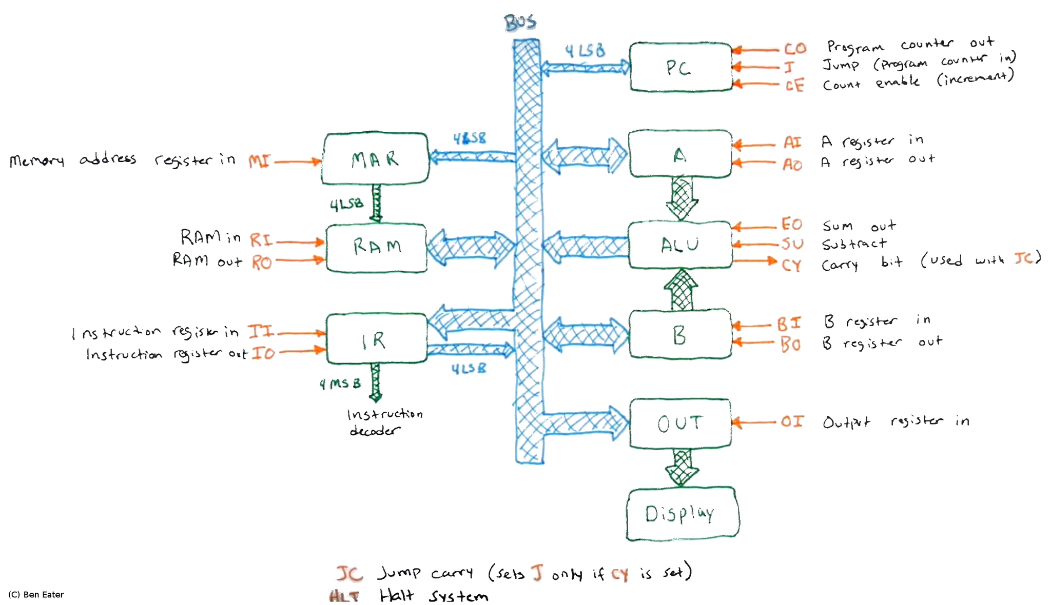
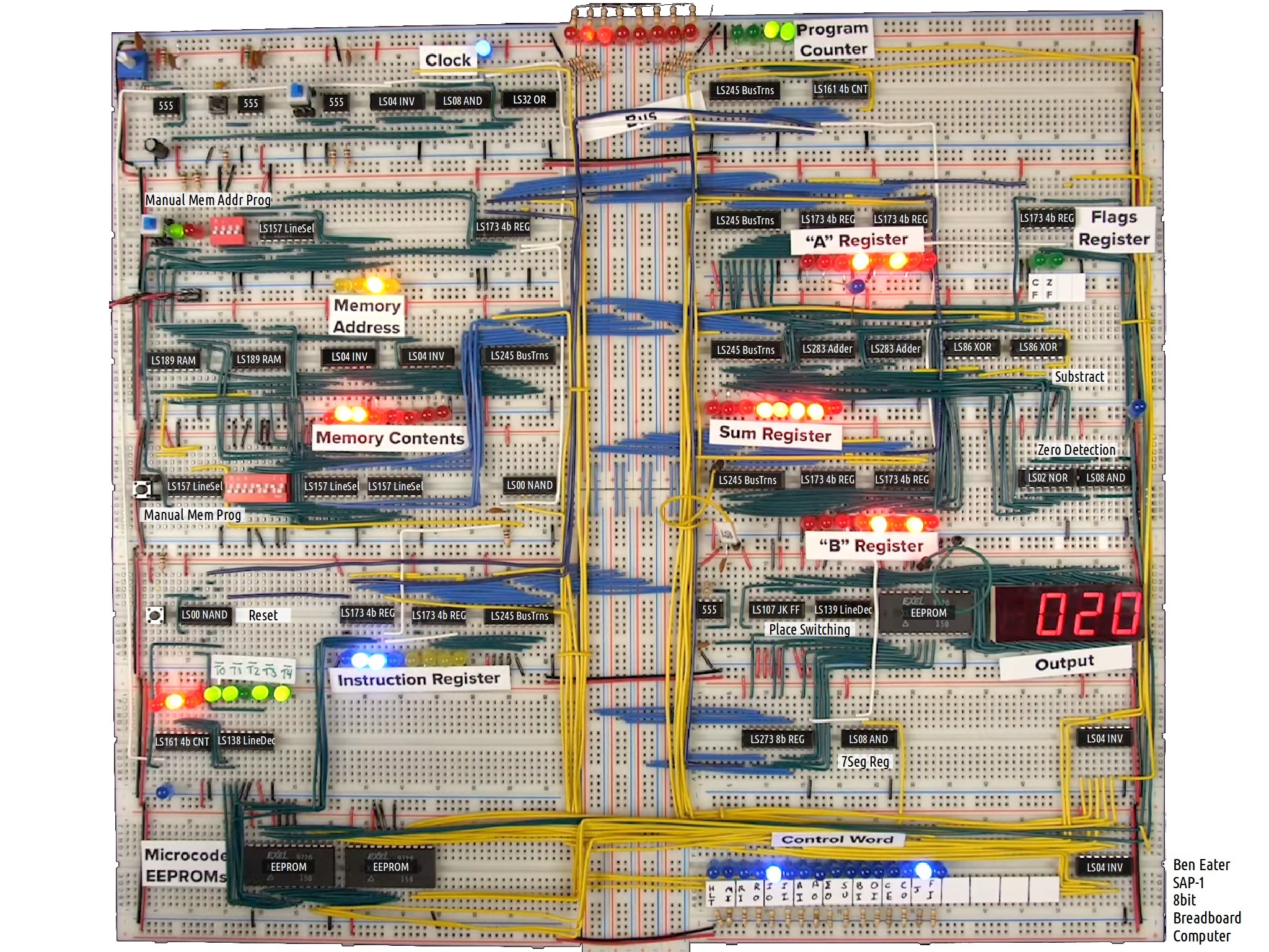
INSTRUCTIONS
The SAP1 is not a real 8bit computer. Important parts are only 4 bits wide:
- Program counter, can only count to 16
- Memory address space is only 16 words, so programs can only be 16 steps long, or even shorter if memory locations are occupied by data
- There are only 16 possible instructions
- The machine code instruction format is:
oooo (4bit instruction) xxxx (4bit address or value)
OPC   DEC HEX         DESCRIPTION
-------------------------------------------------------------------------------------
NOP   00  0000
LDA   01  0001 aaaa   Load contents of memory address aaaa into register A.
ADD   02  0010 aaaa   Put content of memory address aaaa into register B,
                      add A + B, store result in A.
SUB   03  0011 aaaa   Put content of memory address aaaa into register B,
                      substract A - B, store result in register A.
STA   04  0100 aaaa   Store contents of register A at memory address aaaa.
LDI   05  0101 vvvv   Load 4 bit immediate value in register A (loads 'vvvv' in A).
JMP   06  0110 aaaa   Unconditional jump. Set program counter (PC) to aaaa,
                      resume execution from that memory address.
JC    07  0111 aaaa   Jump if carry. Set PC to aaaa when carry flag is set and resume
                      from there. When carry flag is not set resume normally.
JZ    08  1000 aaaa   Jump if zero. As above, but when zero flag is set.
      09  1001
      10  1010
      11  1011
      12  1100
      13  1101
OUT   14  1110        Output register A to 7 segment LED display as decimal.
HLT   15  1111        Halt execution.
Instructions that could be added:
- LDB aaaa - Load content of memory adress aaaa into register B
- STB aaaa - Store content of register B at memory adress aaaa
- ADI vvvv - Add immediate value, but 4 bits only (could save memory)
- CMP aaaa - Compare. Similar to substract but do not update register A, only set zero flag
CONTROLS
01  HLT   Halt the computer
02  MI    Memory address register in
03  RI    RAM in
04  RO    RAM out
05  II    Instruction register in
06  IO    Instruction register out (not needed with 256B RAM mod)
07  AI    Register A in
08  AO    Register A out
09  EO    ALU sum out
10  SU    Switch ALU to substract (otherwise add)
11  BI    Register B in
12  OI    Output in (display bus value on 7segment display as decimal value)
13  CE    Counter enable (increment program counter PC)
14  CO    Counter out (Put program counter value on bus)
15  J     Jump (Counter in = read bus into program counter)
16  FI    Flags register in (store alu flags in flags register)
Controls signals that could be added:
- BO - Register B out (control signal hardware is there, but not used)
- RIC - Reset micro instruction counter (performance gain for instructions with few microcode steps)
Signals from upgrade ideas:
- BRI - bank register in - read address value from bus into bank register
- FPO - output generic bus switches on the bus("front panel")
- GPO - output gamepad buttons latch on the bus
- GPR - reset gamepad latch (could be automatically done by counter?)
- VI - read bus content into video display
- SI - sound input
can be removed: "IO" - We do not need the instruction register out control signal with 256B mod
ASSEMBLY / MACHINE CODE
Tricks
- Substracting 1 from any positive number except 0 will enable the carry bit
Example Programs
Add two numbers
   OPC    VAL     MEMAD   INST VALUE  DESCRIPTION
----------------------------------------------------------
00 LDA    14      0000    0001 1110   Put value "28" from mem addr 14 into A
01 ADD    15      0001    0010 1111   Add value "14" from mem addr 15 to A
02 OUT            0010    1110 xxxx   Output result ("42")
...
14        28      1110    0001 1100   Value 28 in memory
15        14      1111    0000 1110   Value 14 in memory
Add two 16bit numbers (untested)
Add 12473 + 48089
MSB / LSB = most/least significant byte
Notes
- Too long, not possible without register overwriting.
- LDI cannot be used for immediate loading, because it loads 4bit values only.
- No output, 7segment display can only display 1 8bit integer, no place in memory.
Examine output by manual setting memory address register.
   ASSEMBLER      MEMAD   INST VALUE  DESCRIPTION
----------------------------------------------------------
00 LDA    (13)    0000    0001 1001   Load LSB part of 12473 from mem addr 13 in A.
01 ADD    (15)    0001    0010 1111   Add LSB part of 48049, overflow -S> carry is set.
02 STA    (15)    0010    0100 1111   Store result from A into mem addr 15
                                      (Overwrite to save memory, can run only once).
03 JC     (08)    0011    0111 1000   Jump to mem addr 8 when carry is set,
                                      otherwise continue with next instruction.

04 LDA    (12)    0100    0001 1100   Load MSB part of 12473 in A.
05 ADD    (14)    0101    0010 1110   Add MSB part of 48089.
06 STA    (14)    0110    0100 1110   Store result in mem addr 14 (overwrites).
07 HLT            0111    1111 xxxx   Halt the computer, result is in (14,15).
                                      =60562 (1110 1100 1001 0010).
08 LDI    1       1000    0101 0001   Load value "1" (carry) in A
09 ADD    (12)    1001    0010 1100   Add MSB part of 12473 from mem addr 12
10 STA    (12)    1010    0100 1100   Store in mem addr 12
11 JMP    (04)    1011    0110 0100   Jump to addr 04 to finish calculation

12                1100    0011 0000   MSB part of 12473
13                1101    1011 1001   LSB part of 12473
14                1110    1011 1011   MSB part of 48089
15                1111    1101 1001   LSB part of 48089
https://theshamblog.com/programs-and-more-commands-for-the-ben-eater-8-bit-breadboard-computer/
https://bread80.com/2019/09/13/breadboarding-with-diode-logic/
Arduino EEPROM Programmer
https://github.com/beneater/eeprom-programmer
MISC
Python Simulator: https://github.com/LuisMichaelis/Computer-Simulation
Google Calc Spreadsheet Emulator
https://www.youtube.com/watch?v=wB8R0oOkaAw
Upgrades
Full 8 bit mod (256mem locations)
https://www.reddit.com/r/beneater/comments/ad2uko/upgrading_the_ram_module_to_256_bytes/
Also: https://www.youtube.com/watch?v=gqYFT6iecHw&list=PL_i7PfWMNYobSPpg1_voiDe6qBcjvuVui
Parts:
-
Second 74LS161 for 8bit programm counter
-
Memory address register:
-
Second 74LS173 4bit 3state register
-
Second 74LS157 quad 2-input multiplexer (switch output from two 4bit busses) Only neccessary for manual ram programming circuit
-
-
RAM:
-
Before: 74LS189s 64bit ram (16x4) with 3state outputs
-
Replacement: 7130LA35PDG (1Kx8, 9 address lines) dual port static ram
-
-
Microcode has now 2 bytes
-
1 byte instruction, 1 byte data
-
Workflow:
-
program counter out
-
memory address register in
-
memory out
-
instruction register in
-
increment program counter
-
memory address register in
-
memory out
-
actual instructions follow here...
-
-
We do not need the instruction register out control signal anymore!
Instead microcode counter reset?
-
-
Further 16 control signals are rather limiting. 24 would be nicer (=3 eeproms)
Bus control / "Keyboard"
- 8 bus status leds, similiar to SAP1
- 8 switches to form an 8bit word, a bit similar to old computer front panels
- 74LS245 8bit bus transceiver connects the switches with the bus
- Possible control signal: KYI keyboard in
- Could replace SAP1 memory programming circuits
RAM Bank Switching
Assumes 256B mod, would theoretically be possible with 4bit too,
RAM > 256B could be used with bank switching. Different layout would be possible.
Switch complete RAM to other bank
- Add a 8 bit register (bus transceiver 74LS245 + 2x 74LS173) between the bus and the RAM address lines greater than 8. (For 64KB of RAM, for 1KB one 74LS173 is enough)
- New control signal: BRI - bank register in - read value from bus into bank register
- New instruction SBK 0000 0010 - Select/Switch BanK 2
- Would work with ROM too
- Workflow: a long programm could
- Switch to the next bank if near current memory address limit
- Reset the program counter as the PC is relative to the bank
- Proceed at new bank, relative memory location 0, where the next instruction would need to be located
- Cons: No "global" RAM space, banks could not be used for data only, there would need to be instructions too
Bank only a window of the RAM
- We could split the ram e.g. in half and bank the second part.
- Similiar as above, but the banking register would start to control the ram from line 7 instead of 8
- That would leave 128B of "global" ram, and 128B banked (e.g. 7x 128B banks with 1KB RAM)
- Pros: Allows program code to stay in fixed part, and flexible data loading from banks